Semiconductor Failure Analysis Tool
See the Invisible: Pinpoint Defects with Magnetic Field Imaging
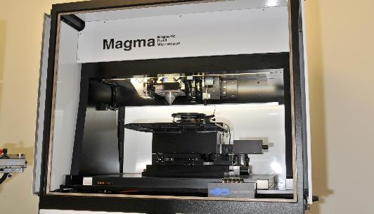
Advanced Semiconductor Failure Analysis with Neocera Magma
What Is Magnetic Field Imaging?
Magnetic field imaging is a powerful way to detect hidden defects in electronic components. When an electric current flows through an IC, it creates a magnetic field. Neocera Magma uses ultra-sensitive sensors to map this field and find issues like short circuits, open lines, or tiny leaks—without damaging the device.
How It Works
| Step | Description |
|---|---|
| 1. Place Sample | Load a chip, wafer, or board into the system |
| 2. Cool Down | Cryogenic system enables sensor performance |
| 3. Scan | High-resolution scanning across the sample |
| 4. Analyze | Software highlights defect locations using magnetic field maps |
Key Features and Benefits
| Feature | Benefit |
|---|---|
| Illumination and Internal Camera | Provides clear visibility during setup |
| Compact Frame | Saves laboratory space and requires a single electrical connection |
| Backside Probing Stage | Allows easy access for complex samples |
| User-Friendly Software | Simplifies setup and speeds up analysis |
| Simplified Cryogenics | Cuts down operating and cooling costs. No liquid nitrogen is required by the system. |
| Large Sample Support | Handles wafers, PCBs, and stacked devices |
| XYZ/Tilt Stages | Enables precise, high-resolution scanning |
| Vibration Isolation | Stabilizes environment and minimizes vibration for more accurate results |
| Ergonomic Design | Easy to use and maintain |
What Can It Analyze?
Magma is designed to analyze a wide range of electronics—from single chips to complex packages:
Wafers (including 300 mm)
Printed Circuit Boards (PCBs)
3D Integrated Circuits (3D ICs)
System-in-Package (SiP)
Stacked Devices
Multi-Chip Modules (MCMs)
Today’s devices are more compact and complex than ever. Neocera Magma helps engineers find microscopic defects early—improving yield, reliability, and performance.
See How Neocera Magma Works
Watch our short video to see how magnetic field imaging helps engineers locate hidden defects in microchips and advanced electronic packages.